New Equipment | Solder Paste Stencils
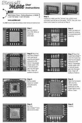
Simplify and Speed Up QFN and LGA device rework. StencilMate™ leadless device rework stencils make the process of reworking leadless devices such as QFNs and LGAs simple and fast. These adhesive-backed poyimide stencils are placed on to the bottom o
New Equipment | Solder Paste Stencils
Step-up / Step-down Stencil. The patented step stencil from LaserJob, called PatchWork® - stencil, was developed to print in one printing step different paste deposit heights. Due to the multiplicity of different component leads on one printed circu
Electronics Forum | Fri Jul 13 19:08:55 EDT 2001 | mparker
Home plate apertures are designed to reduce or eliminate solder balls that occur when placing a chip and reflow of the solder. This aperture type is usually desired when processing with a "no-clean" solder paste. The design of the aperture is usually
Electronics Forum | Wed Jan 08 08:20:52 EST 2014 | emeto
To most of our boards I give 20-30% tolerance in both directions. From experience if you have big aperture on your stencil, the squeegee will scoop certain amount of paste from this aperture and you will see lower height. Depending on your board supp
.JPG)
Used SMT Equipment | SPI / Solder Paste Inspection
The LSM300 follows the successful Laser section Microscopes LSM and LSM2. This new non-contact laser based system is an off-Line solder paste inspection system.LSM300 provides automatic height measurements, eliminating the inconsistencies of manual m

Used SMT Equipment | AOI / Automated Optical Inspection
This AOI was purchased for $49,995 from Manncorp. The Sherlock AOI is in excellent condition and has under 200 hours of usage. The Sherlock AOI Systems detect a comprehensive range of defects and errors in PCB assembly using the Sherlock PCB ins
Industry News | 2003-03-26 08:25:40.0
The QVE00033 transmissive switch's small size, surface mount package and performance make it ideal for noncontact switching applications in disk drives, card detectors, mise and trackballs.
Industry News | 2002-02-04 18:10:34.0
Clean stencils used for backplane, motherboard and other large stencil printing applications
Technical Library | 2023-08-04 15:27:30.0
A designed experiment evaluated the influence of several variables on appearance and strength of Pb-free solder joints. Components, with leads finished with nickel-palladium-gold (NiPdAu), were used from Texas Instruments (TI) and two other integrated circuit suppliers. Pb-free solder paste used was tin-silver-copper (SnAgCu) alloy. Variables were printed wiring board (PWB) pad size/stencil aperture (the pad finish was consistent; electrolysis Ni/immersion Au), reflow atmosphere, reflow temperature, Pd thickness in the NiPdAu finish, and thermal aging. Height of solder wetting to component lead sides was measured for both ceramic plate and PWB soldering. A third response was solder joint strength; a "lead pull" test determined the maximum force needed to pull the component lead from the PWB. This paper presents a statistical analysis of the designed experiment. Reflow atmosphere and pad size/stencil aperture have the greatest contribution to the height of lead side wetting. Reflow temperature, palladium thickness, and preconditioning had very little impact on side-wetting height. For lead pull, variance in the data was relatively small and the factors tested had little impact.
Technical Library | 2024-04-08 15:46:36.0
A designed experiment evaluated the influence of several variables on appearance and strength of Pb-free solder joints. Components, with leads finished with nickel-palladium-gold (NiPdAu), were used from Texas Instruments (TI) and two other integrated circuit suppliers. Pb-free solder paste used was tin-silver-copper (SnAgCu) alloy. Variables were printed wiring board (PWB) pad size/stencil aperture (the pad finish was consistent; electrolysis Ni/immersion Au), reflow atmosphere, reflow temperature, Pd thickness in the NiPdAu finish, and thermal aging. Height of solder wetting to component lead sides was measured for both ceramic plate and PWB soldering. A third response was solder joint strength; a "lead pull" test determined the maximum force needed to pull the component lead from the PWB. This paper presents a statistical analysis of the designed experiment. Reflow atmosphere and pad size/stencil aperture have the greatest contribution to the height of lead side wetting. Reflow temperature, palladium thickness, and preconditioning had very little impact on side-wetting height. For lead pull, variance in the data was relatively small and the factors tested had little impact.

ALPHA® TETRABOND™ is the culmination of "frameless" stencil development; an elegantly simple system designed to enhance the rigidity of the foil, making safe mounting and demounting an easier proposition. Innovatively encompassed in a thin, one piece
Career Center | , | Engineering,Production
Project Management, SMT Process Engineering
Career Center | Theni, Tamilnadu India | Engineering
NPI Engineer: • Playing a role as NPI leader of the Telecom, Aerospace & Server Products to introduce and run to qualify the engineering build from customer. • Conducting Weekly NPI meeting with the CFT team to review the progress of the NPI schedu
Process Development And Characterization Of The Stencil Printing Process For Small Apertures Process Development And Characterization Of The Stencil Printing Process For Small Apertures. The consumers interest for smaller, lighter and higher


